Creating and ordering a custom PCB

I’ve always found something thrilling about circuitboards. I remember the excitement of finding a discarded motherboard on the side of the road as a child, imagining the tiny little electrons flowing in their ordered, angled city.
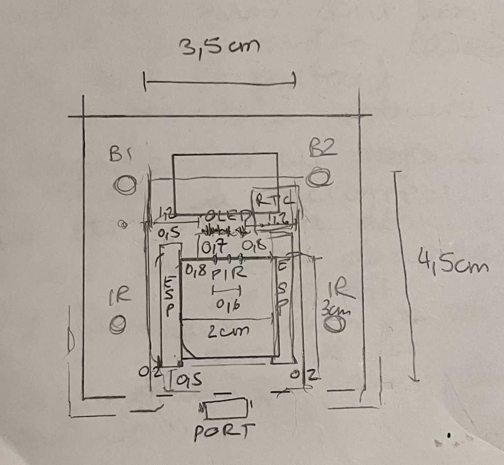
As part of a home automation project, I wanted to house a thermometer, motion sensor and display in a small form factor. A problem I came across was fitting all the modules, board and cables in such a small box!
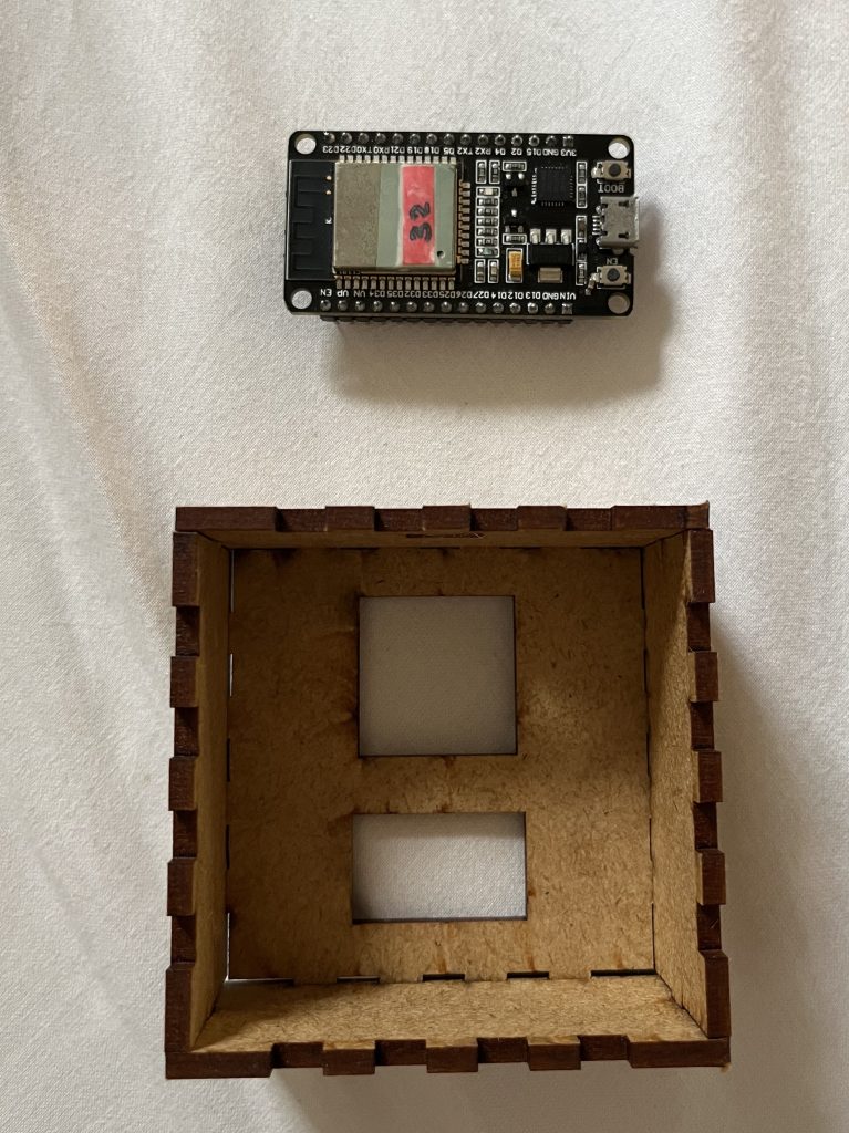
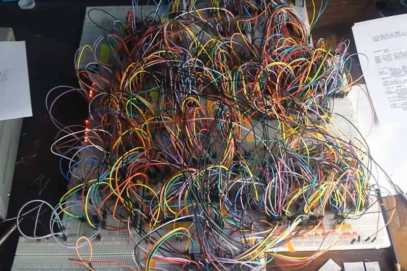
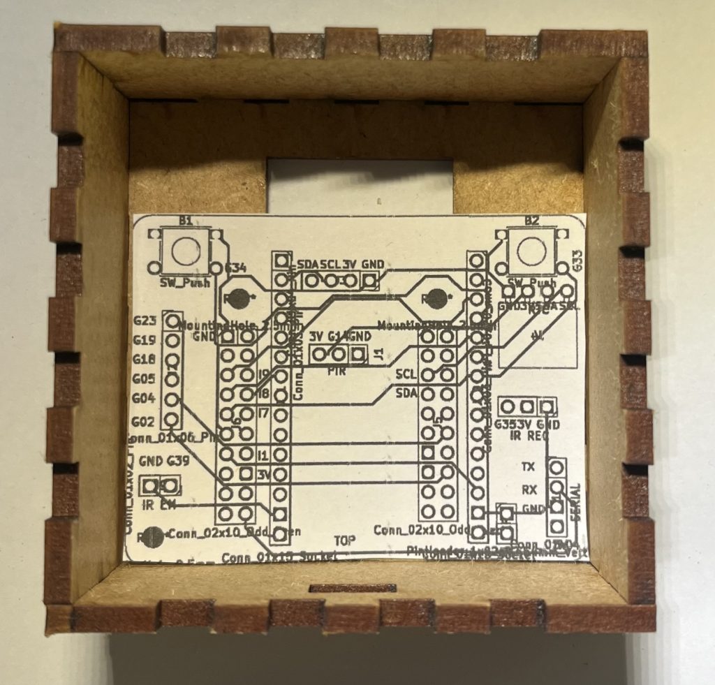
The box I made using boxes.py and an online laser cutting service was only 6x6x2cm on the inside, barely enough to fit in my sensors and screen, let alone free-form dupont cables. It was absolute mayhem.
I decided it was time to try my hand at creating a custom PCB. I've seen people online create their own through online PCB services, and researched the best way to design one.
Software
There is EDA (Electronics Design Automation) software such as Autodesk EAGLE, but the free version being quite limited and the paid version requiring a Fusion 360 subscription, which is upwards of 560 € / year or $630 USD (I know!), that option was quickly thrown out.
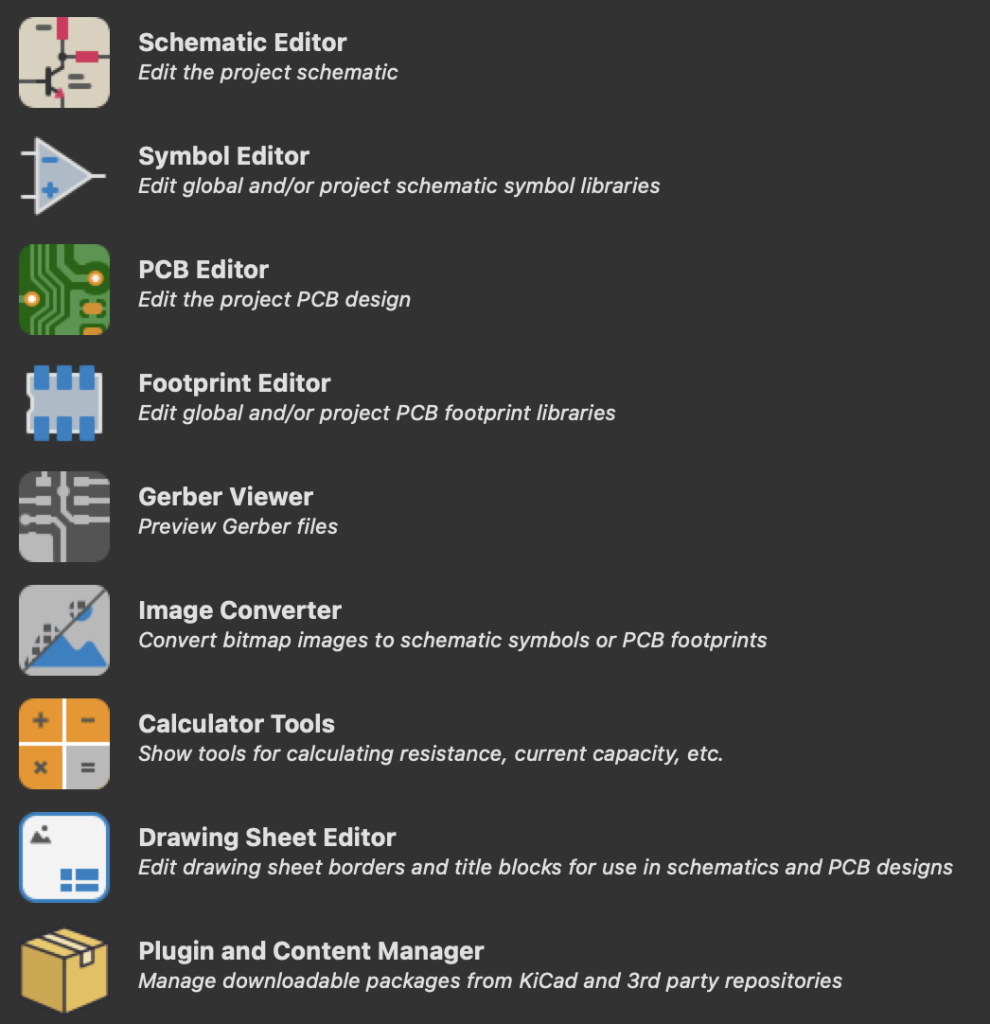
I then came across KiCad, which has checked all the boxes for me. Honestly, it's a godsend. It's an open source PCB design suite that has a wide range of tools from designing circuits to drawing the actual PCB to viewing the model in 3D, to even converting images to PCB-ready footprints! If it even is possible to find something where it lacks, it definitely makes up for it with the vast amount of add-on packages available to install.
As I haven't ever done any digital electronic design, there definitely was a learning curve, but it wasn't very steep.
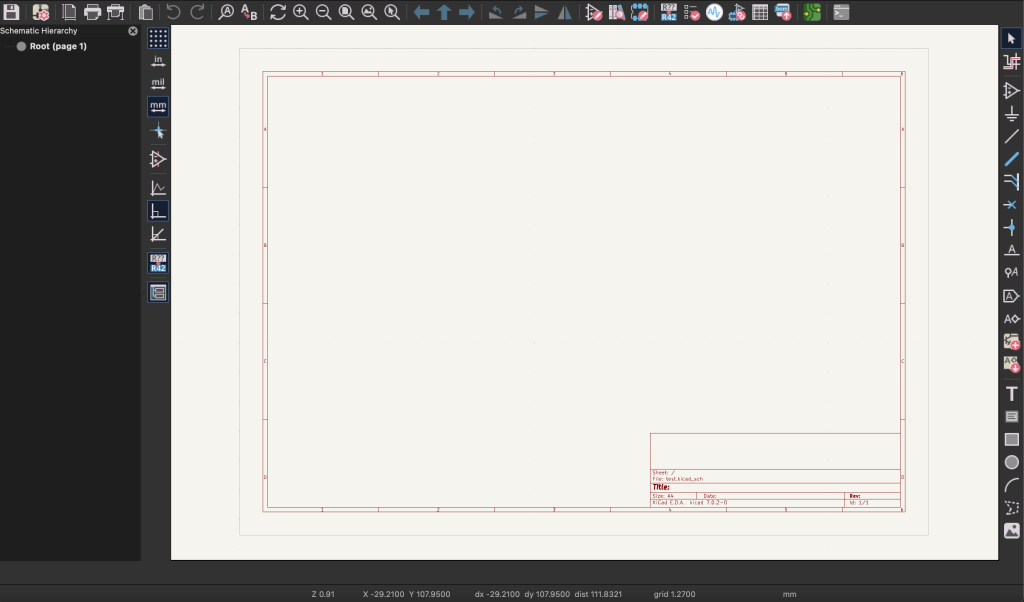
The first thing I did was to create a new project in KiCad, which initializes files for circuitry and PCB layout. This step is important if you want to create schematics and then design them onto a PCB, which you can't do if you create a separate schematic or PCB file. I then opened up schematic editor. For a newbie, the amount buttons and information may be a little overwhelming at first but it quickly starts to feel comfortable.
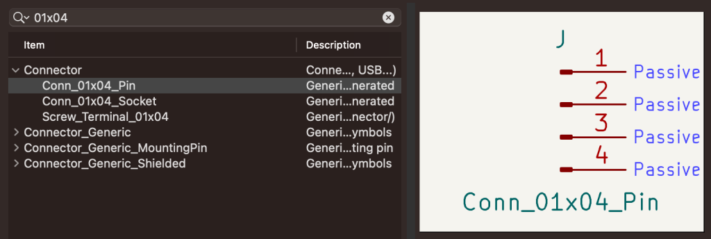
After a bit of googling, I found the "insert component" button on the top of the right sidebar, which seemed like a good place to start. The software then prompted me to select the component I wanted among its huge library (I never once had to fetch a component from an external library). For example, you can insert a 1×4 connector by typing "01×04" in the search bar.
After adding all the components I needed for my project (mostly connectors to join all my modules up), it was time for me to specify the wiring between the components. There are two ways of doing this: The first way is to select the "add wire" icon ("W") on the right, and join two or more pins, but this is tedious and the shapes you define won't make it to the final PCB as this is just a schematic. The other way is to label pins, and KiCad automatically joins up pins with the same label. There is a scary amount of label types that can be added, but I just selected the first option and hoped for the best, which worked in my favor.

Something I had to look out for was the fact that the labels have to properly join up with the pins for them to be recognized.
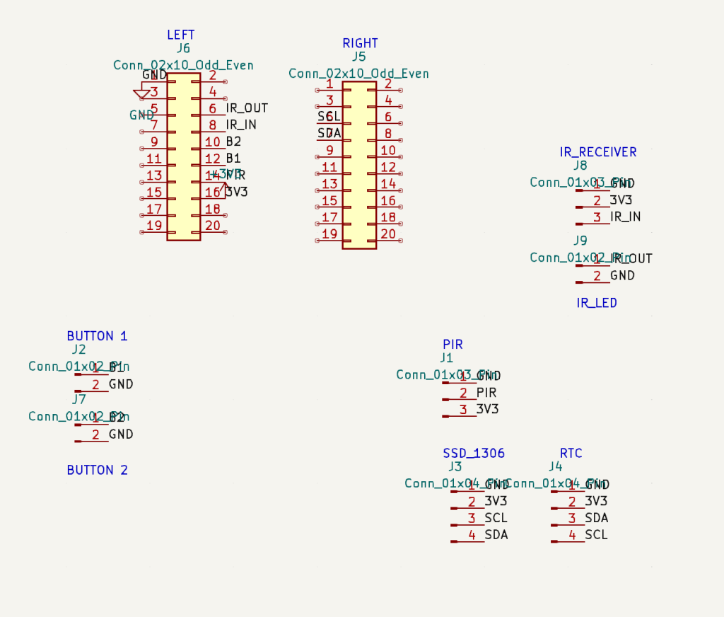
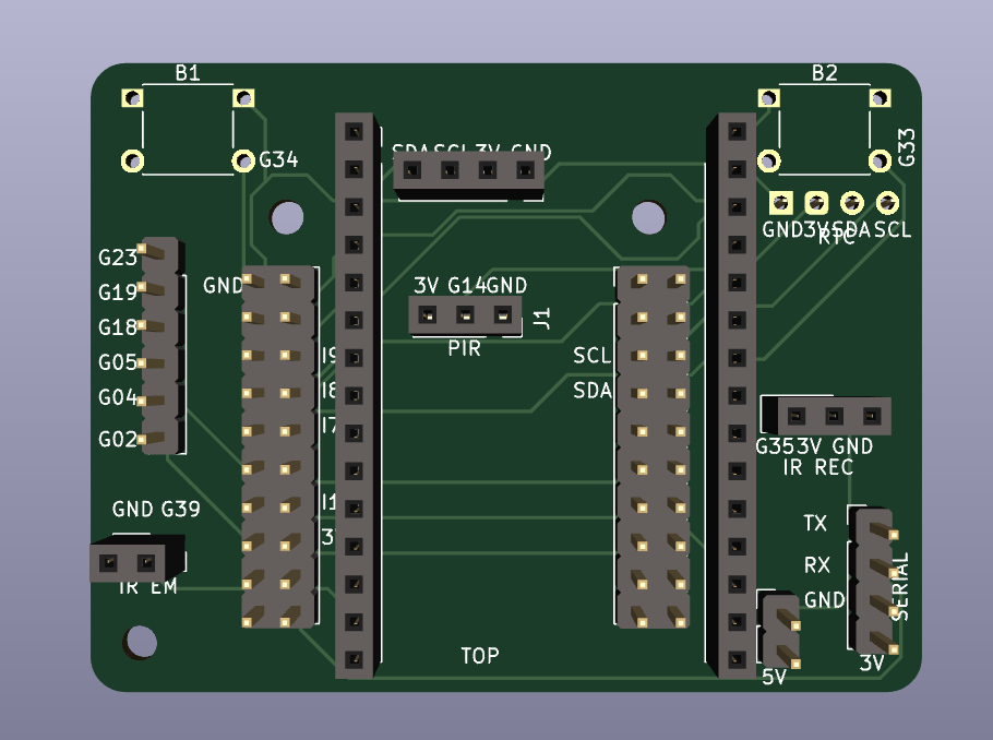
I wanted to build a circuit to fit an ESP32 D1 mini, an I2C RTC/Temp sensor, an I2C oled screen, PIR and IR receiver/emitters so I could use a remote with my device. I added components with the right number of pins while making sure that the pin order was correct.
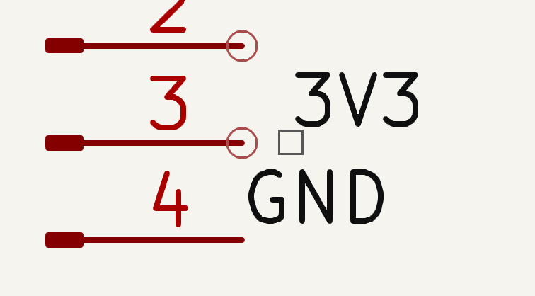
Once I had my circuit done, there were a few things left to do: KiCad gets upset if you don't define power symbols, so I selected "Add Power Symbol" ("P") and added the power and ground pins for my circuit (3.3V and GND in my case). Once you do that, you get a symbol to add to a pin just like any label. This defines that pin, and all the ones with the same label, as belonging to that power symbol.
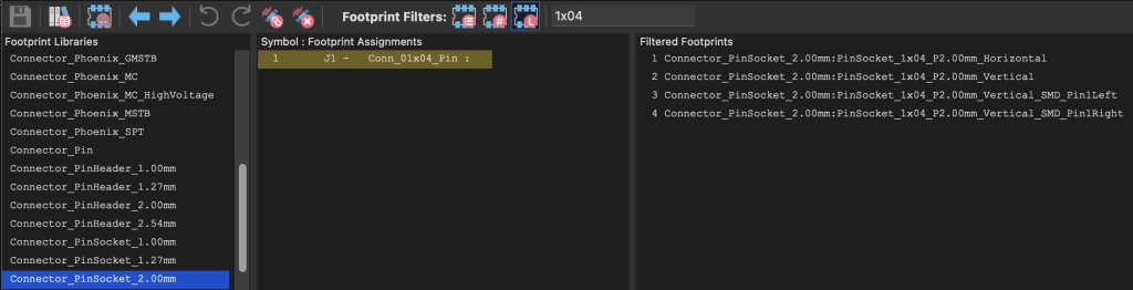
Another thing to do is to define footprints for all the components – this gives the software an idea of how the component looks like in the real world. To do this, click on the "Run footprint assignment tool" button on the top bar, and it opens a list of the components in the schematic in the middle and a list of available footprints to assign on the left. Unassigned components are highlighted in yellow, and then it's a matter of selecting the right footprints. For connectors, you can choose a "connector" or a "header" configuration. The default header/connector size is 2.54mm (This works with dupont cables and Arduino/Espressif boards). For example, if I wanted a 1×4 pin connector to map out to a 1×4 header, I'd select the Connector_PinHeader_2.54mm family on the left, and search "1×04" on the top bar (Note: don't type "01×04" as connector footprints don't have a leading "0" like components do). Once you find the right configuration, double click on it.
Building the PCB
After assigning all the footprints on my circuit, I went to the "Tools" tab bar and selected "Update PCB from Schematic". This sends the circuit to the PCB builder, ready to start building a physical circuit. At first the components are haphazardly placed out onto the screen, and the circuits jumbled about (don't worry – the PCB isn't going to come out like that and I will get to the tracing later) but you can move them about to place them. This is where the measuring tools and grid comes in handy: I went to Settings>Display Options>Full window crosshair so that I could make sure components were aligned when I moved them. I would select each component, align it, and measure by pressing the space bar to reset the "dx" and "dy" properties on the bottom of the screen: these let you see how much your cursor moves to properly space out components. Another tool is the Dimension tool: after selecting the User.Comments layer on the right, you can click between two points to show the distance between them, this is useful for later reference.
Something that seems trivial but that is important to make sure your PCB comes out the way you envisioned it is drawing diagrams. This helps make sure you get your spacing, number of components and orientation right.
Once everything is positioned to taste, it's time to create a shape for the PCB. This is known as edge tracing. I clicked on the "Edge.Cuts" layer (in the layer list on the right) and then selected the line tool on the right toolbar to create a square around my PCB. There are other tools such as the arc tool to create rounded edges.
A note on pads:
There are two main types of pads (the plated surfaces on which components are mounted) in KiCad: Through-hole which is a hole that penetrates the entire thickness of the board and SMD (Surface Mount Device) which is just a plated surface that doesn't come with a drilled hole.
It's time for the last building stage: creating traces, or wires, between components: The easiest way to do this, especially for a simple PCB with few components, is to use an auto tracer. This algorithmically determines the traces to join up pins the same way the schematic is laid out. I downloaded a plugin called "Freerouting" that does precisely this. You may need to install/update Java to make this work like I did. In the PCB editor, select Tools>External Plugins>Freerouting from the menu bar. This launches the tool and automatically traces on the front and back PCB layer.
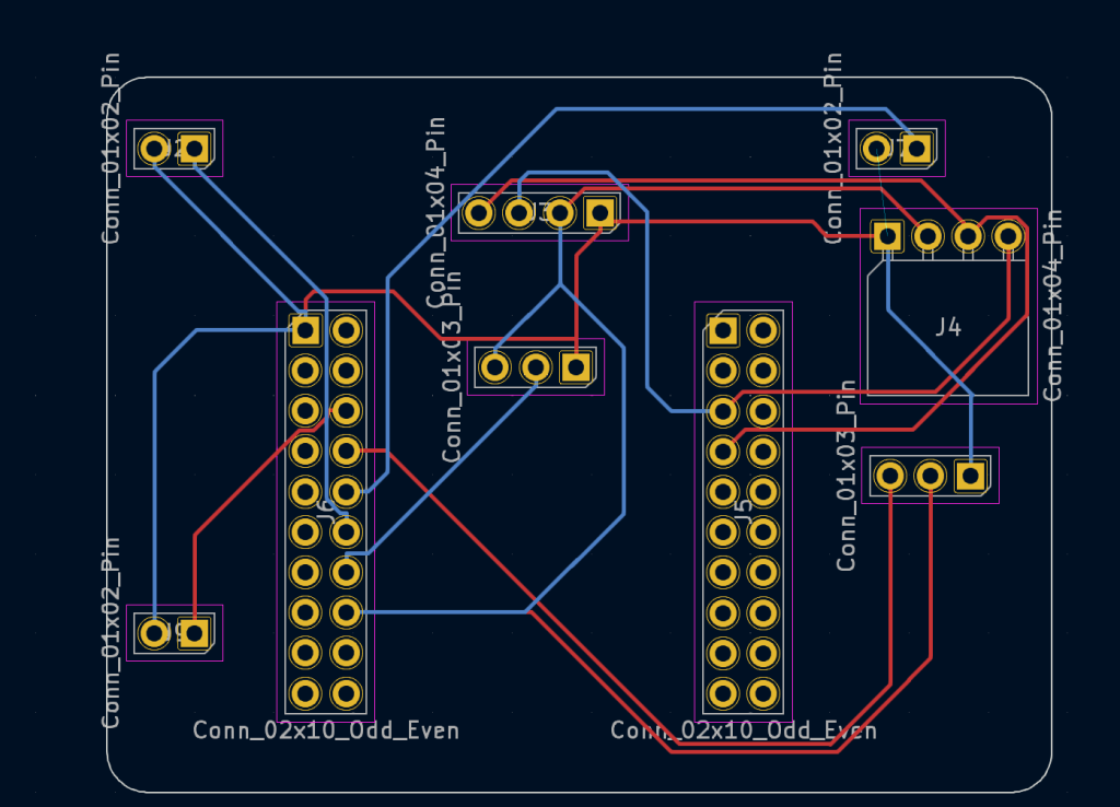
There were a few traces I wasn't happy with, so I modified them by selecting the layer on which the trace is on (either F.Cu – front or B.Cu – back), deleting the traces I want to change, and selecting the "Route Tracks" tool ("X"). This handy little tool avoids traces which aren't part of the circuit and does things like 45º angles (This is important for high-frequency signals which bounce back off the corner of 90º angles). There are a few things to consider when tracing: The front and back are obviously electrically isolated so front and back traces can intersect but not traces on the same side. Pins traverse the entire board so this is a useful place to join traces from different sides to the same circuit, and if you want to do this without a pin you can make a hole, called a "via" which does this (This adds holes to drill so avoid if you want to keep costs down).
One can also add labels to components that will be printed out onto the PCB, this is known as a "Silkscreen". Select the silkscreen layer (front or back) in the layers list and you can place text or shapes onto it. Make sure that the silkscreen doesn't overlap with any pads as they will get clipped. The silkscreen is printed on top of the traces so having them overlap isn't an issue.
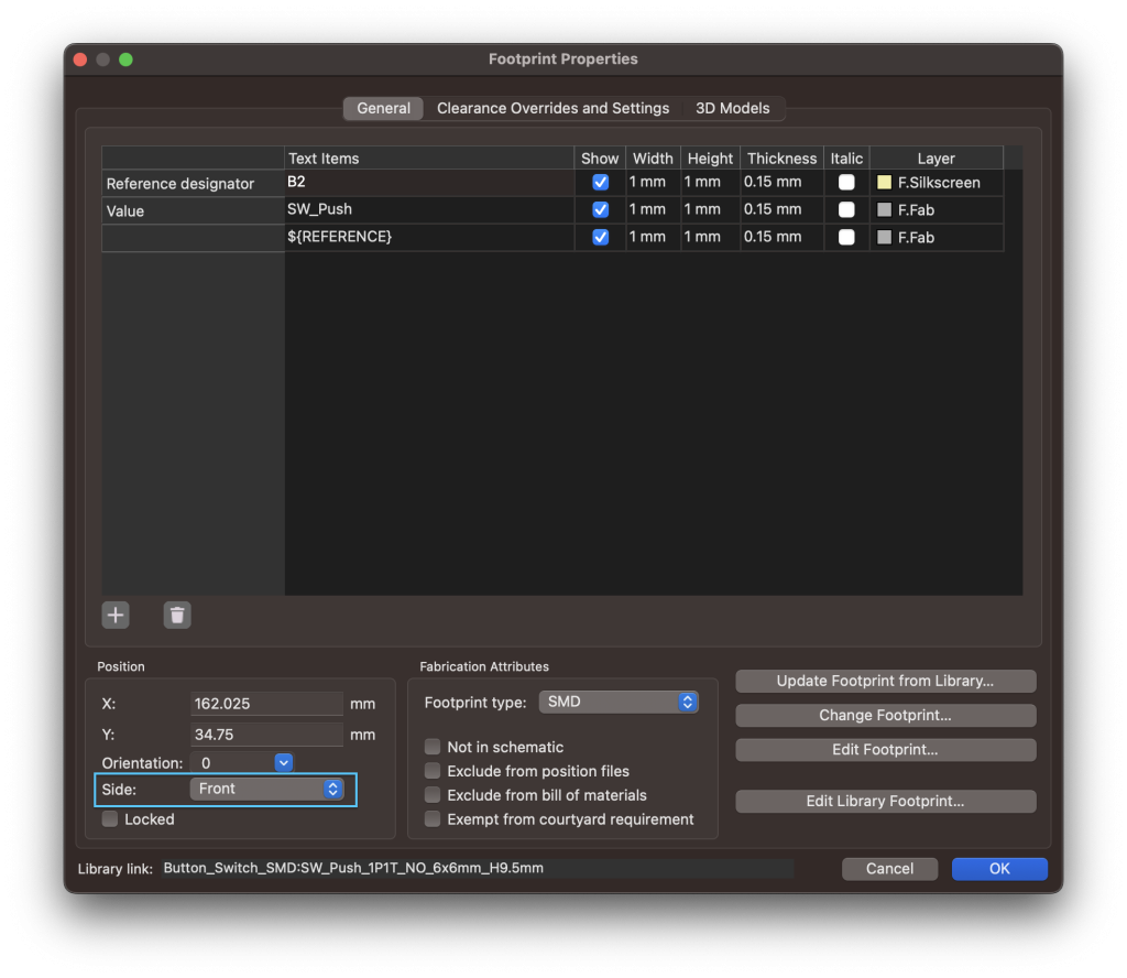
Another thing I found tricky was to switch the side of components: You can mount components on either side, and although for through-holes it doesn't change much (As the pads which go through the thickness of the board are symmetric on both sides), for surface-mounted components it makes a huge difference: By double clicking a component to make the footprint properties dialog come up, you can select the side it's mounted on in the "position" section.
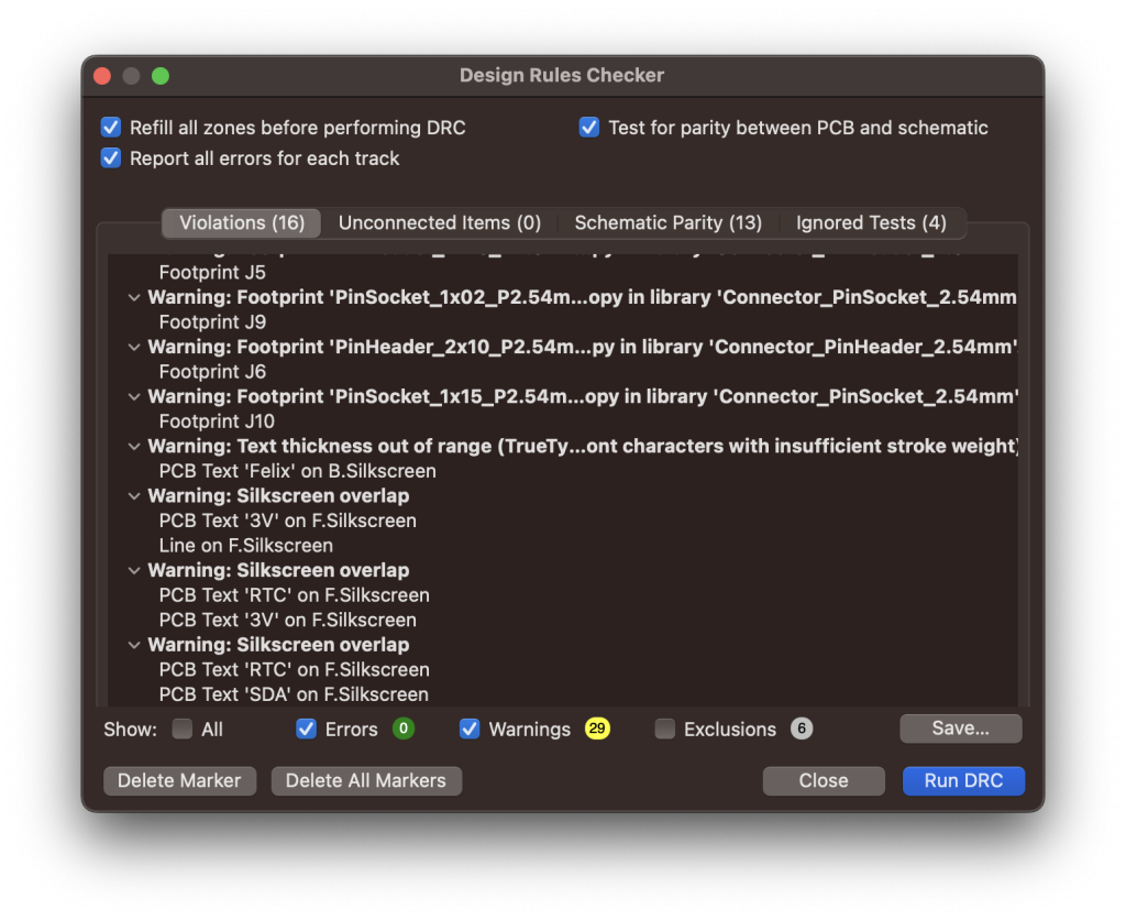
The next step is to make sure there aren't any issues with the design: PCBs must follow a DRC (Design Rule Check) to make sure board edges are properly defined, different traces/components don't intersect... This is done by clicking on the "DRC window" icon on the top bar, and selecting "Run DRC". If it finds any issue, it will put arrows in the PCB diagram and selecting the error in the window highlights the component and lists the error. I had a few issues with overlapping labels and unconnected pads, but they were quickly resolved.
After everything is in order, select View>3D viewer (Option-3) to get a rendered view of the PCB. I find that this helps with mentally representing all the components in space, and making sure everything is how you envisioned it. Seeing the front and back traces separately also helps to make sure the pads are wired optimally.
Before ordering, I suggest printing the PCB onto a piece of paper, this is to make sure everything fits in the right place so there's no surprise when you get your real PCB! You can easily do that in KiCad by going to File > Print and selecting the layers you want.
Ordering
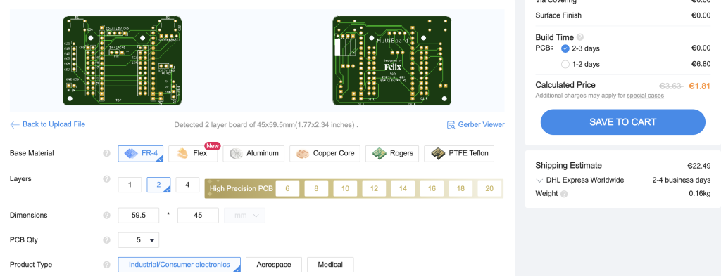
It's time to order the PCB! To get the file ready for export, choose File>Plot.... There are 4 things to export: Traces (front and back), Masks (font and back), Silkscreen (Front and back), and the drill holes. To export drill holes, go to "Generate Drill Files...". I found it best to select the "PTH and NPTH in single file" so that you get one simple file for all the drill holes. Select "Generate drill File" and "Plot" on the dialogs, and it should export the gerber files in the same folder as the KiCad project.
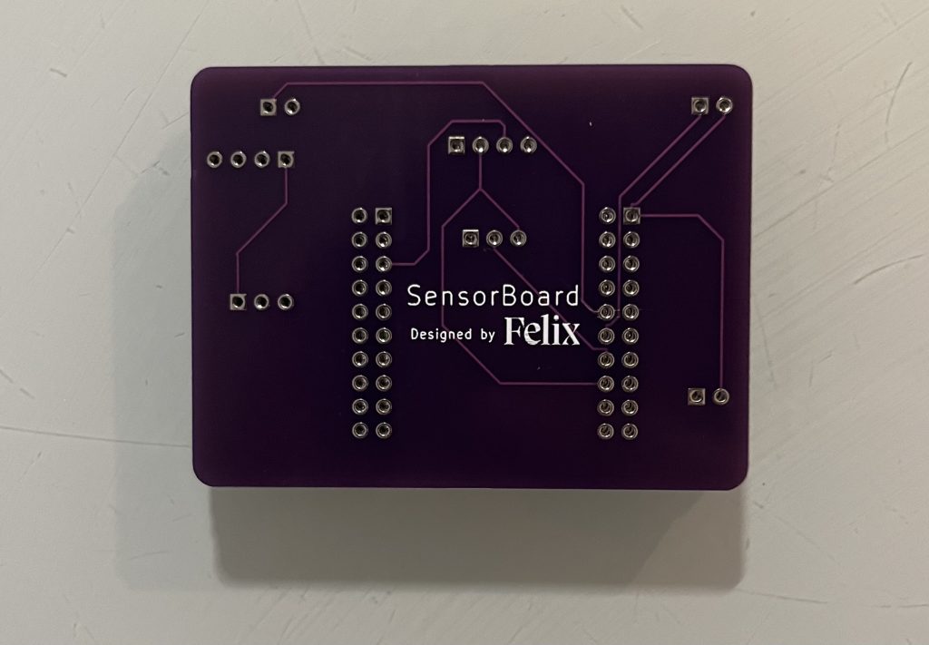
I researched a few online PCB ordering services: PCBWay, JLCPCB and AllPCB are based in China, while OSHPark is USA-based. After looking at reviews and comparing prices, I found that the best way to go was PCB way, especially for a hobby project. To upload the KiCad model, I zipped a folder containing all the gerber files and uploaded it on the website. It automatically populated the fields for me, and it was just a matter of selecting the PCB color I wanted (I went with purple) as well as the delivery service. As the minimum order for most PCB manufacturing services is 5 boards, I got the idea of modifying my board so that it could fit an ESP32 DevKit as well, and so that I could use the I2C and various pin support as well for other projects, unfortunately I got that idea after I had ordered my PCB and it was too late to change.
The ordering process was quick, and I could see on my order history the stage at which my board was, from drilling to plating to cutting.
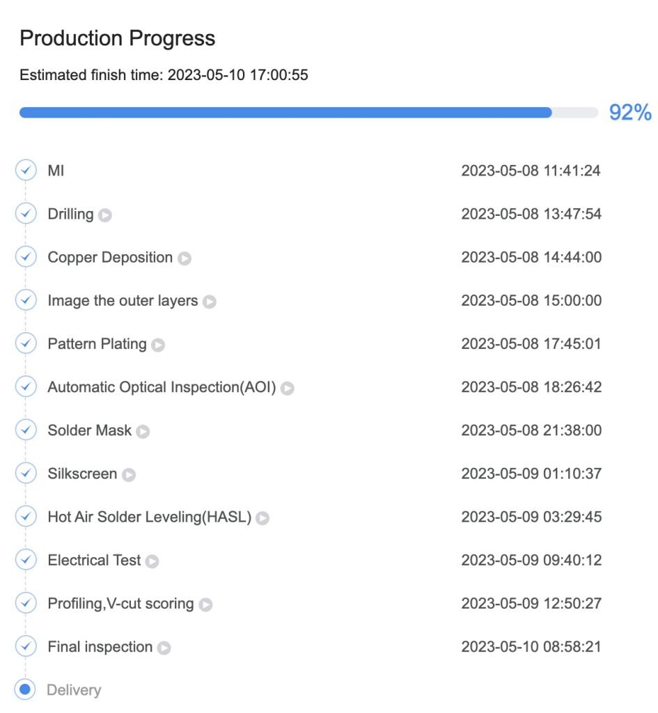
The board came within 10 days from ordering, I was very impressed with the speed! I got a pack of 5 boards in purple, and I'm quite pleased with the quality of the board, from the thickness to the screen printing resolution. I was warned by KiCad that the font used for my name wasn't of uniform thickness, but JLCPCB handled it very well.
The verdict
Overall, I'm quite happy with the design process with KiCad, as well as the quality of service offered by JLCPCB. Although I do feel bad about not supporting local businesses and ordering PCBs from across the globe, the price, especially for a hobby project, made it a no-brainer for the quality of the finished product. Receiving your own creation in the mail is such a rewarding feeling!
If I was to do anything differently next time, I would definitely add drill holes which would have made mounting it easier, I would also take the time to think about what other project the board could be used for given the minimum order amount of 5.
KiCad, FTW!